Transmission electron microscopy
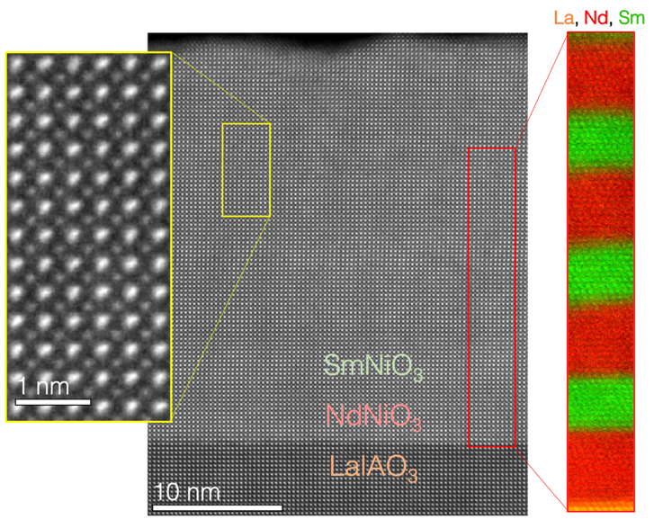
Aberration-corrected scanning transmission microscopy (STEM) is one of the most used techniques for characterization of the crystal properties of perovskite oxide heterostructures [1,2]. By using an angstrom-sized probe, we can scan crystals, lattice defects or interfaces and extract information about their structural, chemical and electronic properties directly in the real space with sub-atomic resolution [3–5].
We use a Thermofisher Titan Themis 60-300 kV, equipped with a Cs double corrector DCOR (CEOS), an X-FEG and a monochromator, to characterize the structural, chemical and electronic properties of the oxide heterostructures that are fabricated in Geneva. This advanced microscope is located in the interdisciplinary center for electron microscopy (CIME) at the EPFL campus (Lausanne)
This work is conducted in collaboration with Dr. Duncan Alexander from the Electron Spectrometry and Microscopy Laboratory (LSME) group.
[1]. J. Gázquez et al., Materials Science in Semiconductor Processing. (2017)
[2]. M. Varela, J. Gazquez, and S. J. Pennycook, MRS Bull., (2012)
[3] . P. D. Nellist and S. J. Pennycook, Ultramicroscopy, vol. 78, no. 1–4, (1999)
[4] . P. D. Nellist, “Scanning Transmission Electron Microscopy,” in Springer Handbooks, (2019)
[5] . R. F. Egerton, Electron Energy-Loss Spectroscopy in the Electron Microscope. (2011)
Main researcher
Chih-Ying Hsu, Duncan Alexander